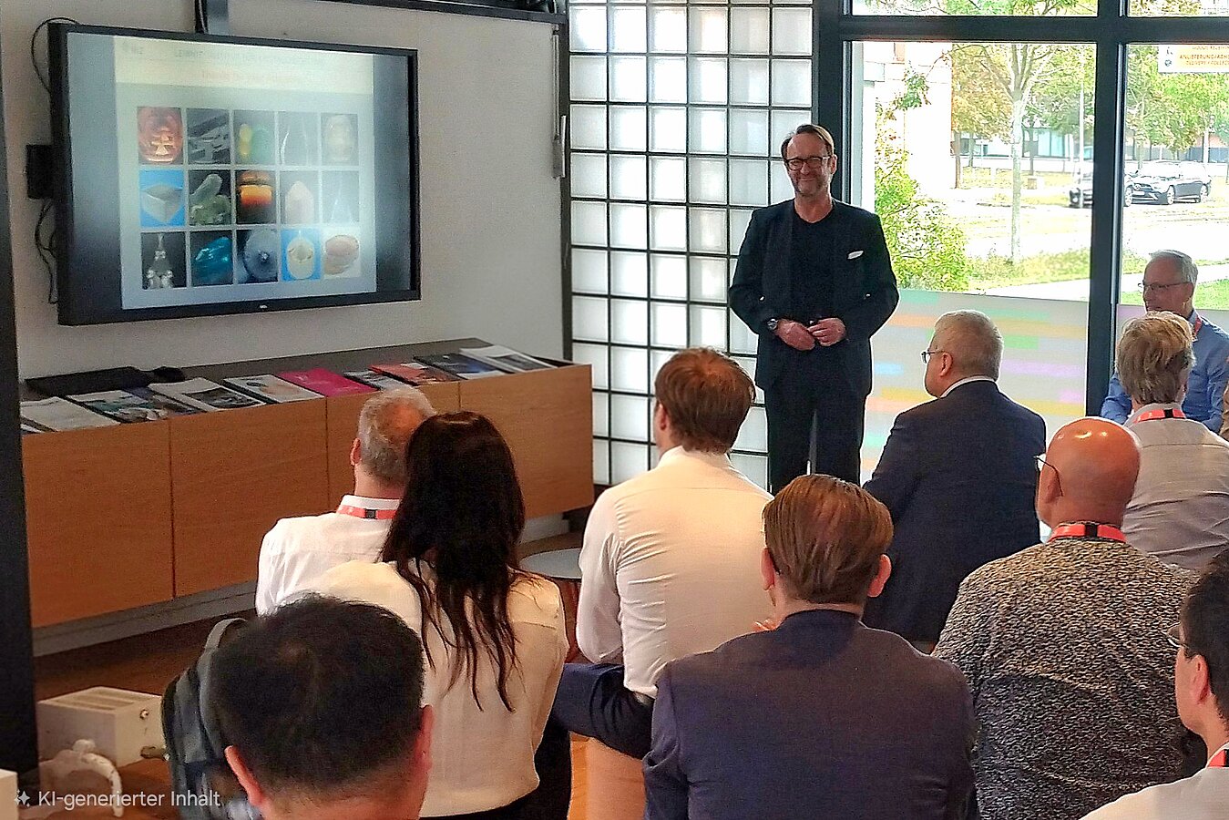
The innovation mission, titled “Advanced Packaging, Testing, and Integrated Photonics”, took place from September 28 to October 2, 2026, with stops in Berlin and Dresden. It was organized by the Netherlands Innovation Network and the Netherlands Enterprise Agency (RVO) in collaboration with the ChipNL Competence Centre, PhotonDelta, and PhotonicsNL. The mission aimed to strengthen ties between Dutch and German research institutions and companies and explore opportunities for joint research and development activities.
The delegation brought together experts from across the semiconductor and photonics sectors. Participants represented organizations working in integrated photonics, semiconductor technology, electronics, precision manufacturing, and test and measurement technology. Representatives from innovation support organizations and the financial sector also took part.
Insights into research at IKZ
The visit began with a presentation by the Dutch Photonic Integration Technology Centre (PITC), an initiative led by the research organization TNO in collaboration with academic and industry partners. The center focuses on advancing integrated photonic technologies and supporting their industrial application.
IKZ Director Prof. Dr. Thomas Schröder and Dr. Christian Kränkel, Head of the Center for Laser Materials, then introduced the institute and its research activities. Their presentation highlighted the development and production of crystalline materials for semiconductor technology and photonics, as well as their potential for future applications.
During the subsequent laboratory tours, the guests had the opportunity to see crystal growth processes at IKZ firsthand. Divided into two groups, they visited the semiconductor growth hall and the oxide crystal growth area. The tours were led by Prof. Dr. Thomas Schröder and Prof. Dr. Matthias Bickermann, Deputy Director of IKZ.
Exchange on shared research interests
Beyond the laboratory visits, the meeting provided an opportunity to discuss different technological approaches and research interests. The overlap between crystal growth, semiconductor technology, and integrated photonics offers several areas of shared interest and potential for further exchange.
The visit formed part of the broader innovation mission, which sought to strengthen scientific and technological ties between Germany and the Netherlands and identify opportunities for future collaboration.
Contact:
Leibniz-Institut für Kristallzüchtung (IKZ)
Prof. Dr. Thomas Schröder
Director
Phone: +49 (0) 30 / 246 499 117
Email: sekikz-berlin.de
Web: https://www.ikz-berlin.de
Stefanie Grüber
Press and Public Relations
Phone: +49 (0) 30 / 246 499 126
Email: stefanie.grueberikz-berlin.de

